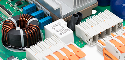
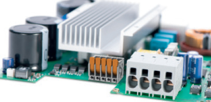

The increasingly compact design in electronics development today means that power and signal connections are now combined on the same printed circuit boards. The resulting increase in power density changes how we think about the requirements for PCB connection technology.
Everything seems to have become smaller in recent years: take the computer, for example. At the turn of the millennium, a home PC stood at around 24 inches deep, but over the years, while the functionality of the internal hardware has grown, the hardware itself has shrunk to the point that nowadays the same computer could be notepad sized and comfortably carried in a pocket. The situation is similar for industrial machinery and equipment electronics: they too are shrinking. A prime example of this is in motor controls. In the past, primitive and space-intensive contactor circuits were required, whereas today the motor, gearbox and inverter form an intelligent and powerful unit at a fraction of the size.
This development has also had a residual effect on power electronics, as used in drives or inverters. The structural separation of the signal level and the power level having long since been abolished, the components mounted on the circuit boards are also becoming increasingly smaller. Because of this, they can be placed closer together – with constant or even increasing connection power. This seeming paradox has had a profound influence on the way we view PCB design and connection technology.
Increased Function
Today’s PCB terminals, while compact, must reliably carry high currents in a safe and efficient manner. At the same time, those connectors must be able to withstand demanding environmental conditions, such as extreme vibration or fluctuations in temperature. Not only that, but electronic developers are increasingly pressured to keep an eye on bottom line profitability as well.
In terms of connection technology, this means that while price considerations are certainly important in themselves, the total installed cost of PCB terminals in terms of functional connection integrity is also increasingly important. An installation that is either over- or under-designed has subtle, hidden costs and liabilities. Therefore, it is essential that connections are sized to fit the scope and scale of the overall application. A prime consideration therein is wire gauge. High current connectors come in a variety of ranges for nominal cross-sections of 10, 8 or even 4 AWG (4 mm², 6 mm² and 16 mm² respectively) to accommodate voltages up to 600 V (UL) / 1000 V (IEC) and current up to 72 A (UL) / 85 A (UL).
The introduction of spring pressure technology in PCB terminal blocks has further increased connection reliability and universal usage, which equates to added cost-savings. Whereas in the past, legacy screw terminations required cumbersome calibration and adherence to torque requirements, push-in or tool-actuated spring pressure technology assures a reliable contact every time regardless of the installer (and without the time-consumptive need to ever retighten).
This choice of terminals can be further delineated by determining the primary end installation type. Terminal blocks for PCBs that are intended to be factory wired can be selected from a wide range of cost-effective push-in or tool-actuated options. Where the end installation is to be done primarily in the field, new lever-actuated variants offer tool-free, end-user convenience. It is vital to note, however, that designers only select lever-actuated terminal blocks that offer clearly visible indication of opened/closed status. Some terminals may appear to be closed visibly when they are in fact not fully actuated. This opens the dangerous possibility of loose wires, faulty connections and disaster. It is essential therefore to select lever-actuated terminal blocks that are binary in operation, i.e., either fully opened, or fully closed – and unambiguously so.
Safe and Easy Access
In addition to connection reliability, high current, spring pressure PCB terminal blocks offer some special advantages when it comes to saving space. Since tool operation and test access can occur in the same direction and orientation as conductor insertion, terminals can be conveniently placed and operated even with the particularly dense placement of other individual components on the printed circuit board. This makes these types of terminals ideal for external device connection – for example, if spring pressure terminal blocks are designed to protect against direct contact with a distance of > .118 inches (3 mm), they are then suitable for use as housing feedthrough connections in electric power drive systems with adjustable speed according to UL 61800-5-1: 2012.
Ease of Use
In addition to space requirements, fast wiring is an important labor-saving factor in ensuring the shortest possible assembly times. Developers who choose push-in or tool-actuated PCB terminal blocks can save considerable installation time by directly inserting (pushing in) solid conductors and fine stranded conductors with ferrules or by taking advantage of tool-actuation technology for stranded and fine stranded conductors without ferrules. Either connection method consistently enables safe, secure wiring within seconds.
If individual assemblies are only prepared – but not wired – by the manufacturer and are later wired in the field for end-use operation, a comfortable and unambiguous operability of the connection is possible through the use of the previouslymentioned lever-actuated PCB terminal blocks. The compact dimensions and high current carrying capacity of these terminals, coupled with intuitive and tool-less handling proves to be particularly user-friendly and fast. As stated previously, it is extremely important that the respective locking positions (open / closed) are clearly visible and representative of the true state of the connection, however. It is also important that the force of the open spring ensure that the lever closes with little effort and therefore a secure contact of the terminal is always made. Errors in handling with these types of terminals are virtually impossible while maintaining speed of installation.
Flexibility of the Design Process built-in
When designing PCB circuits, designers often do not consider the requirements for connection technology in the early stages of the design process. Frequently, terminals are chosen as simply and inexpensively as possible only after the main functionality of the circuit board has already been realized. This often means that connection components must be able to be integrated into the overall design with a high degree of flexibility. Therefore, designers require a full terminal block portfolio to be available that offers the possibility for conductor connections to be made either horizontally or vertically to the printed circuit board and that also allows for testing possibilities at 0 ° and 90 ° angles in relation to the connection direction.
For lever-actuated versions in the designer’s toolkit, there can be some added flexibilities implied. For example, some terminals are designed so that when the lever is in the fully open position, it is at an angle (approximately 60 ° to the terminal, for example) that allows for convenient operation even when the conductor connection is vertical to the printed circuit board. In these cases, because the open lever is not physically touching – nor anywhere near – the circuit board or its components, the contact can be closed comfortably thus minimizing the risk of damaging the circuit board. Additionally, the space beneath the lever – even when open – remains free for additional electronic components, such as SMD resistors.
Having a product range that fully meets the demands of power electronics today; designers can assure that they are giving themselves the ability to combine compact dimensions, high current carrying capacity and convenience in wiring with a particularly high degree of design freedom.
Conclusion:
Modern devices increasingly need compact components, but this constantly evolving miniaturization process demands a lot from electronics, including the connection technology. Modern PCB terminal blocks must be correspondingly compact and powerful at the same time. In addition, high-quality products are characterized by a high degree of user-friendliness and offer great flexibility for the future of PCB design.
Portions of this WAGO White Paper previously appeared in a different form in a German publication as written by WAGO Product Managers, Mike Knobel and Viktor Dick.
Text: CORY THIEL, WAGO
Photos: WAGO